The BJT: Why a Small Base Current Commands a Large One
August 2026
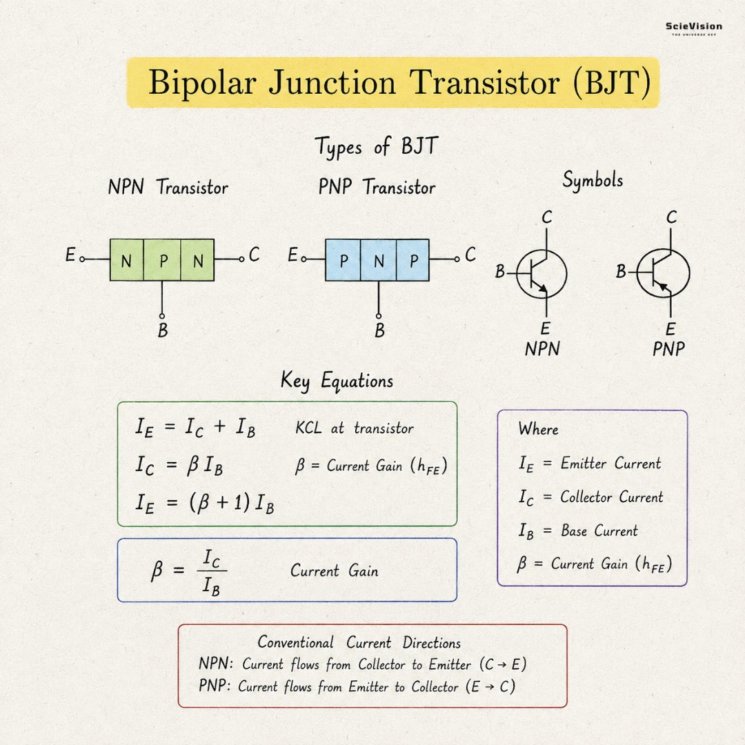
Source chart: @scievision369 on X, 2026-08-05. Every equation, symbol and current direction on the chart itself was checked against standard device-physics references and all of them hold — including the two conventions most often drawn backwards. The surrounding post is a genuine long-form explainer, though its opening list leans hard on a hedge: “Without the BJT, there would be no smartphones, computers, televisions, satellites, or the internet as we know it.” Television, computers and satellites all existed before the transistor — the BBC’s regular high-definition service opened in November 1936, eleven years before the point-contact device — so “as we know it” is carrying the sentence rather than decorating it.
This picks up where Electronics Fundamentals — and a Real Roadmap for Learning Them leaves off. That page argues for learning the math underneath electronics rather than around it, and points at a first lesson on voltage, current and resistance. The bipolar junction transistor is a natural next step: it is the first active device most people meet — the point where a beginner’s circuit stops being resistors and capacitors, and Kirchhoff’s current law gets applied to something that can amplify.
What the chart gives you, and what it doesn’t
The chart states the relationships correctly:
$$I_E = I_C + I_B \qquad I_C = \beta I_B \qquad I_E = (\beta + 1) I_B \qquad \beta = \frac{I_C}{I_B} = h_{FE}$$
The first is Kirchhoff’s current law applied to a three-terminal device — everything in equals everything out. The third follows from the first two. (One convention note the chart inherits from nearly every textbook: $h_{FE}$ with capital subscripts is the DC current gain $I_C/I_B$, while the small-signal gain used in AC analysis is $h_{fe} = \partial I_C / \partial I_B$. They typically differ by 10–30%.)
What no reference card tells you is why $\beta$ exists at all, or what sets its size. That is the only genuinely interesting thing about a BJT.
Why a small base current commands a large collector current
Take an NPN. Three layers, and the differences between them are the whole trick:
- The emitter is the most heavily doped region — often above $10^{20}\ \text{cm}^{-3}$.
- The base is extremely thin and much more lightly doped — typically around $10^{18}\ \text{cm}^{-3}$, and only a fraction of a micron across.
- The collector is lighter still — ten times lighter than the base in a fast integrated BJT, and a hundred to ten thousand times lighter in the discrete and power parts most readers will actually handle — and physically the largest. Light doping lets the base–collector depletion region spread into the collector, which is what allows the device to stand off a large reverse voltage without punching through the base. Its size is about dissipating heat.
Forward-bias the base–emitter junction and electrons pour from the emitter into the base. Almost all of them diffuse straight across and are swept into the collector by the reverse-biased base–collector junction. That is the collector current, and it is the easy part.
The interesting question is the other one: what is the base current, and why is it so small?
The base current is everything that goes wrong
$I_B$ is not a small copy of $I_C$. It is the sum of the ways the process leaks. Three main ones:
- Holes injected backwards from the base into the emitter. A forward-biased junction conducts in both directions — electrons go one way, holes go the other. Only the electron half is useful. This is normally the largest of the three terms, and it is the reason the emitter is doped so much more heavily than the base: the ratio of the two currents goes as $N_E/N_B$, so to first order, making the emitter a hundred times more heavily doped cuts the wasted hole current by about a hundred. Only to first order — at the doping levels real transistors use, that promise is not kept, for a reason we come back to below.
- Recombination in the base. Some injected electrons meet a hole before they get across. Each one consumes a hole that must be resupplied through the base terminal. Because the base is far thinner than the distance an electron typically travels before recombining (a base width $W_B$ of order 0.1–1 µm against a diffusion length $L_n$ of order a few to a few tens of µm), this term is small.
- Recombination inside the base–emitter depletion region. Small at normal currents, but it falls off more slowly than the useful current as you turn the device down — which is exactly why $\beta$ sags at low collector currents.
The two suppression mechanisms have names. Emitter injection efficiency $\gamma$ is the fraction of the junction current carried by the useful carrier — it handles term 1. Base transport factor $\alpha_T$ is the fraction of injected electrons that survive the trip — term 2. (Term 3 sits outside this decomposition, which is part of why $\beta$ misbehaves at low currents where term 3 matters most.) Together:
$$\alpha = \gamma \, \alpha_T \qquad\qquad \beta = \frac{\alpha}{1 - \alpha}$$
What actually limits β — and why the obvious calculation overshoots
This is worth working out, because the obvious calculation gives an answer that is far too generous.
Base transport alone gives $\alpha_T \approx 1 - W_B^2 / 2L_n^2$. Put in a realistic $W_B = 0.5\ \mu\text{m}$ and $L_n = 10\ \mu\text{m}$:
$$\alpha_T = 1 - \frac{0.25}{200} = 0.99875 \quad\Rightarrow\quad \beta \approx 800$$
A typical good $\beta$ is around 100. So base recombination alone does not explain where $\beta$ lands: if it were the only loss, everything built to this geometry would sit near 800, and ordinary parts are specified an order of magnitude below that. Something else is doing the limiting, and it is term 1. The standard expression for the back-injection-limited gain — $\beta_\gamma$ alone, not the whole story (Hu, Eq. 8.4.5) — is a product of four ratios, not a single one:
$$\beta_F \;=\; \frac{D_B}{D_E}\cdot\frac{W_E}{W_B}\cdot\frac{N_E}{N_B}\cdot\frac{n_{iB}^2}{n_{iE}^2}$$
The three losses combine reciprocally, $1/\beta = 1/\beta_\gamma + 1/\beta_T + 1/\beta_{SCR}$, so the smallest one wins. With $\beta_T \approx 800$ from above and $\beta_\gamma \approx 100$, back-injection accounts for the overwhelming majority of the base current.
But no single factor inside $\beta_\gamma$ is the villain either — the design is hemmed in from several sides at once, and that is the more useful thing to know:
- The diffusion constants and widths “cannot be changed very much,” in Hu’s phrase.
- The obvious lever is a large $N_E$ and a small $N_B$. But $N_B$ cannot go too low without raising base resistance, which wrecks high-current and high-frequency performance.
- And pushing $N_E$ up stops paying. At very heavy emitter doping the bandgap narrows, which raises $n_{iE}^2$ and eats the gain you bought: raising $N_E$ from $10^{19}$ to $10^{20}$ does not buy a factor of ten.
That last constraint is why the heterojunction bipolar transistor exists — build the emitter from a wider-bandgap material and the $n_{iB}^2/n_{iE}^2$ term improves directly, without needing an emitter doping that defeats itself.
The consequence: β is a yield, not a gain
The base current is not a small version of the collector current. It is the waste stream of the same process — the back-injected holes, the electrons that recombined, the pairs lost in the junction.
$\beta$ is the ratio of what got through to what was lost.
A transistor genuinely does multiply — both current and power. That is exactly what makes it an active device, and it is why $I_C = \beta I_B$ is a useful thing to write down. What it does not do is create energy. The collector current is drawn from the supply; the base signal only steers it. So “current gain” is not wrong, it is just misleading about the source: it invites you to picture the base signal being enlarged, when what actually happens is that a very light touch on the base releases current the supply already had. A valve, not a multiplier — even though the numbers multiply.
A large $\beta$ means an efficiently built transistor, not a powerful one.
Two things that follow, and matter in practice
1. β is designed for, but it cannot be held to tolerance. Process engineers absolutely do target a $\beta$ — base width and doping ratio are engineered to hit it. The problem is sensitivity: $\beta$ depends on the base width, the hardest dimension in the device to control, and it drifts with temperature and with collector current (term 3 above). A 2N3904 is specified 100–300 at 10 mA. An unsuffixed BC547 is specified 110–800 — a 7:1 spread on one part number — which is exactly why the family is sold in graded bins (BC547A 110–220, B 200–450, C 420–800) so a designer can buy a narrower window. Any circuit whose behaviour depends on a specific $\beta$ works on the bench and fails in production, which is why real amplifier stages use emitter degeneration and feedback to make the result depend on resistor ratios instead — quantities you can buy to tolerance.
2. The current model is a consequence, not the governing law. Collector current is set exponentially by the base–emitter voltage:
$$I_C = I_S\, e^{V_{BE}/V_T}\left(1 + \frac{V_{CE}}{V_A}\right)$$
with $V_T = kT/q \approx 25.7$ mV at 25 °C. The $V_{CE}$ term is the Early effect, and it is what gives the transistor its finite output resistance. $I_C = \beta I_B$ is not a rival model — it is what falls out when $\beta$ happens to be roughly constant. The base current is simply what the base terminal must supply to sustain the $V_{BE}$ that the exponential demands. Both pictures are useful; the current one is easier to design with, and the voltage one is what shows that $\beta$ was never the governing quantity to begin with — which is the real reason it refuses to hold still.
NPN and PNP
Same physics, layers and currents reversed: a PNP swaps every semiconductor type, and holes become the injected carrier. The chart draws both symbols correctly, including the convention that trips up nearly everyone — the emitter arrow points outward on an NPN and inward on a PNP — and gives conventional current as collector-to-emitter for NPN and emitter-to-collector for PNP, also right.
The symmetry is not perfect, though. Holes in silicon are roughly three times less mobile than electrons, so a PNP built to the same geometry ends up slower and typically lower-$\beta$ than its NPN counterpart. That asymmetry is why discrete and integrated designs lean NPN wherever they can.
Catalog status: Proven Systems
Nothing here is in dispute — the physics is standard textbook material; only the emphasis, on which loss actually limits $\beta$, departs from the usual telling. Bardeen and Brattain demonstrated the first point-contact transistor at Bell Labs in December 1947; Shockley conceived the junction transistor — the device on this page — in January 1948, published its theory in 1949, and saw the first working one built in 1950. Everything above is standard semiconductor device theory. No PBT connection is claimed and none is needed.
References
- Chenming Hu, Modern Semiconductor Devices for Integrated Circuits, ch. 8 — free chapter PDF, UC Berkeley. Source for $\beta = \alpha/(1-\alpha)$ (Eq. 8.4.4), the back-injection-limited $\beta_\gamma$ (Eq. 8.4.5), the Gummel-number picture, the doping figures, and the emitter band-gap narrowing argument. Note Hu treats base recombination as negligible and does not use the term base transport factor — that decomposition comes from reference 2.
- M. J. Gilbert, ECE 340 Lecture 34: Intro to the BJT — III — University of Illinois. Source for the classical $\gamma$ / $\alpha_T$ decomposition and $\alpha = \gamma\alpha_T$. Works out back-injection and base recombination explicitly (for a PNP); it does not cover the depletion-region term.
- Computer History Museum, Invention of the Point-Contact Transistor (1947) Conception of the Junction Transistor (1948), and 1951: First Grown-Junction Transistors Fabricated — Teal and Sparks began growing them in April 1950; Bell Labs announced the advance on 4 July 1951.